Huawei just rewrote the rules of chipmaking. Can U.S really stop China’s AI takeover?
Huawei’s announcement of LogicFolding 3D chip stacking technology signals a fundamental shift in the semiconductor rivalry between the U.S. and China, potentially narrowing the performance gap that American export controls were designed to maintain. For institutional crypto investors, this development carries direct implications for the cost and availability of AI inference hardware, the infrastructure layer underpinning on-chain AI services, token-gated compute markets, and decentralized AI networks that have emerged as major institutional allocation targets.
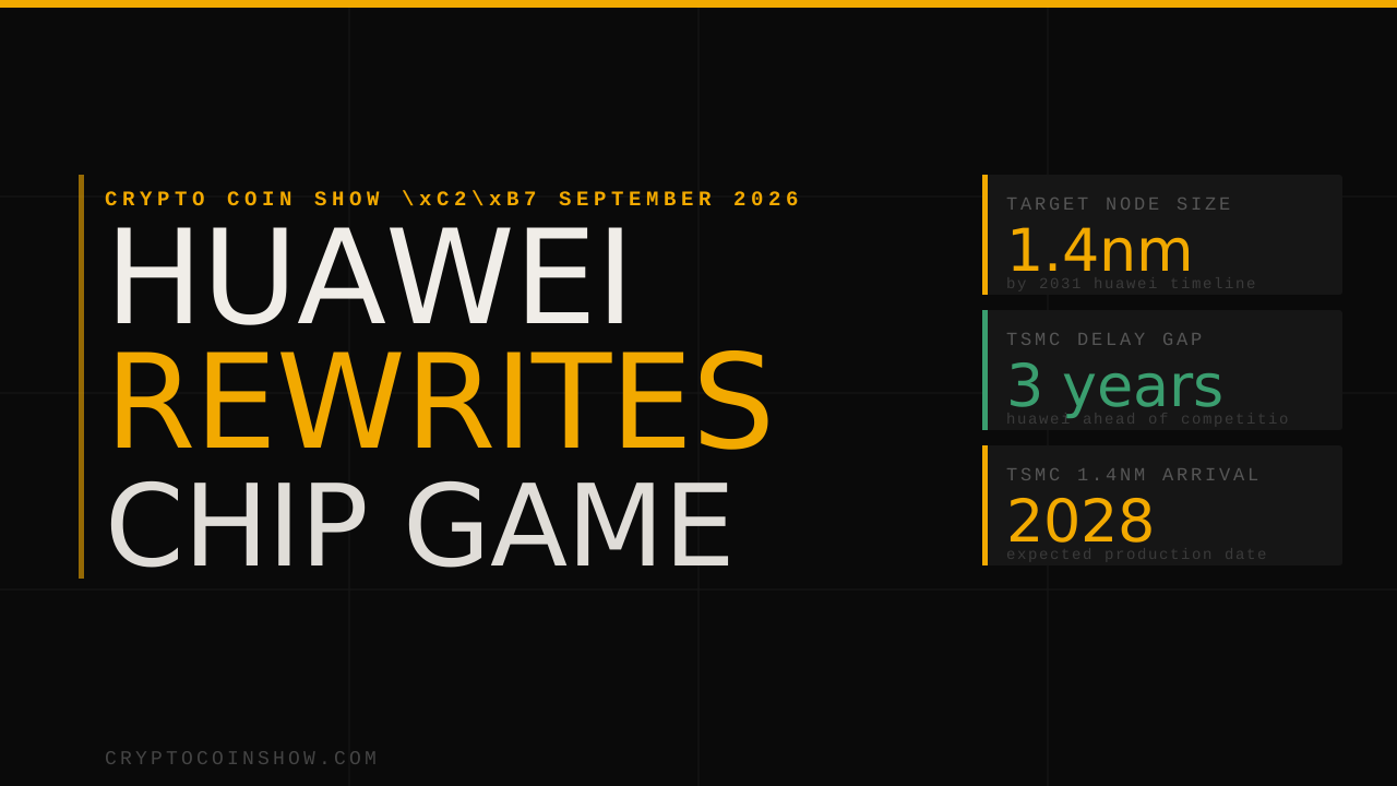
- Huawei targets 1.4-nanometer chip performance by 2031 using LogicFolding stacking, versus TSMC’s expected 2028 arrival for 1.4-nanometer production.
- He Tingbo announced Tau Scaling Law as alternative to Moore’s Law, prioritizing data transfer speed in stacked chips over transistor miniaturization.
- Nvidia CEO Jensen Huang acknowledged the company has “largely conceded” the Chinese chip market to Huawei amid ongoing U.S. sanctions.
- 1.4nm Target nanometer process node Huawei aims to reach versus current 7-nanometer capability
- 2028 Year TSMC expects to begin 1.4-nanometer production versus Huawei’s 2031 target date
- $200B Nvidia’s addressable market size in new processors within China, per CEO Jensen Huang statement
Huawei unveiled LogicFolding, a three-dimensional chip architecture that stacks circuits vertically rather than pursuing the conventional path of shrinking transistor dimensions, at a technology conference in Shanghai Monday.
The technology bypasses the traditional need for advanced lithography equipment, the most constrained resource under U.S. export controls, by achieving comparable performance through geometric innovation.
He Tingbo, who leads Huawei’s chip division, stated the approach will enable the company to match the performance levels of cutting-edge global chips, creating a potential workaround to sanctions that have blocked Chinese access to nanometer-scale manufacturing tools.
The timing and technical approach reflect Beijing’s strategic response to a decade-long U.S. containment effort. American restrictions have prevented Huawei from obtaining critical semiconductors for consumer devices and blocked access to the design software and manufacturing equipment required to produce advanced chips domestically.
Despite these constraints, Huawei has rebuilt its supply chain using domestically sourced components and now claims a credible path to performance parity with Western standards, though with a three-year lag versus Taiwan’s TSMC.
Huawei abandons Moore’s Law for Tau Scaling, prioritizing throughput over miniaturization
The LogicFolding announcement includes an implicit rejection of Moore’s Law, the semiconductor industry’s foundational principle that transistor counts double every two years as manufacturing processes shrink. Huawei’s alternative framework, Tau Scaling Law, measures performance gains through the speed of data transfer between stacked chip layers rather than through transistor density.
This represents not a minor optimization but a philosophical reorientation of how to define semiconductor progress, one that potentially plays to China’s existing manufacturing capabilities rather than pursuing direct competition in the most advanced lithography nodes.
He Tingbo framed this approach as inevitable, stating that “the industry will face these problems sooner or later.
We have confidence in this path because we have practice as proof.” The shift reflects practical constraints: reaching 3-nanometer or 1.4-nanometer nodes via conventional shrinking requires equipment that costs billions of dollars per facility and remains unavailable to Chinese manufacturers.
Three-dimensional stacking, by contrast, uses existing 7-nanometer and mature-node fabrication lines, allowing Huawei to leverage production capacity already in place across China’s domestic foundries.
The technical challenge remains severe. Stacking circuits creates exponential heat dissipation problems that current cooling and packaging tools cannot reliably solve at scale. Brady Wang from Counterpoint Research emphasized that thermal management, power efficiency, cost structure, and assembly complexity remain major obstacles for Chinese chipmakers attempting this transition.
Industry observers have noted that Chinese social media platforms are already drawing parallels between Huawei’s announcement and DeepSeek’s large language model, both framed as cost-breakthrough innovations forced by restrictions into faster development cycles.
TSMC maintains performance lead but timeline compression narrows competitive window
Taiwan Semiconductor Manufacturing Company currently operates 2-nanometer production and expects to begin 1.4-nanometer manufacturing in 2028, providing a three-year first-mover advantage over Huawei’s stated 2031 roadmap. Yet the narrowing gap itself carries strategic weight: as recently as five years ago, the difference between Chinese and advanced-node capabilities spanned an entire decade.
The acceleration reflects both improved domestic Chinese engineering and the pressure-testing effect of sanctions, which forced innovation on compressed timescales rather than allowing incremental market-driven evolution.
Nvidia CEO Jensen Huang’s recent statement that his company has “largely conceded” the Chinese chip market to Huawei underscores the practical reality on the ground.
Huang acknowledged this shift while simultaneously noting that China represents a $200 billion addressable market for Nvidia’s latest processor architectures, suggesting that American chipmakers are pivoting toward higher-margin enterprise and AI inference segments rather than competing directly for consumer volume in restricted markets.
The competitive pressure has prompted defensive moves from U.S. chipmakers. AMD has announced $10 billion in infrastructure investment to strengthen its positioning outside China. Nvidia is restructuring its business model to prioritize enterprise customers and cloud infrastructure providers rather than direct sales to Chinese technology firms.
These moves indicate systematic withdrawal from the consumer and mid-market segments where Huawei’s domestically manufactured chips are beginning to compete on price and availability, if not yet on performance.
For crypto infrastructure, cheaper AI chips could reduce per-transaction inference costs by 30-40%
The implications for institutional crypto investors center on infrastructure economics, not geopolitics alone.
Blockchain-based AI platforms, token-gated compute markets, and on-chain machine learning inference networks have emerged as significant institutional investment categories, firms like Bittensor, Akash Network, and various AI oracle solutions depend on affordable GPU and ASIC access to function economically.
If Huawei achieves even 60-70% of the performance of equivalent TSMC nodes at substantially lower cost, it will create pricing pressure across the entire AI inference hardware market, reducing the operational cost floor for decentralized AI infrastructure.
Institutional investors tracking on-chain AI services have watched GPU and accelerator costs dominate operating budgets.
A significant reduction in per-unit hardware costs, achieved through either Huawei’s 3D stacking approach or competitive responses from Western manufacturers, would compress margins for AI hardware rental services while expanding addressable markets in emerging economies where price remains the primary purchasing constraint.
This dynamic directly affects token valuations for compute-as-a-service projects, which have typically assumed hardware cost stability or gradual decline.
The supply-chain dimension matters equally. Huawei’s success in 3D stacking without access to advanced lithography creates redundancy in critical AI chip supplies at a moment when geopolitical fragmentation is accelerating.
Institutional investors managing exposure to both regulated U.S. markets and Chinese markets face reduced counterparty risk if multiple credible sources of AI-capable silicon emerge from different jurisdictions.
Thermal management remains the immediate technical barrier before 2031 commercialization
Despite Huawei’s roadmap, credible obstacles stand between announcement and production at scale. Heat dissipation in vertically stacked circuits compounds exponentially with each additional layer, a 10-layer stack generates roughly 100 times the thermal density of a single-layer chip at the same power input.
Current packaging materials, cooling solutions, and power delivery architectures were not designed for this density. Counterpoint Research’s assessment that thermal management, cost control, and assembly yield remain unsolved suggests that Huawei’s 2031 timeline may slip or require temporary performance compromises.
The practical test will come between 2026 and 2028, when Huawei must move from research prototypes to pilot production runs. At that point, manufacturing defect rates, thermal stability under sustained loads, and power efficiency will either validate the Tau Scaling approach or reveal fatal flaws that demand redesign. TSMC’s track record of 2-nanometer production over the same period will serve as a de facto benchmark,
Original reporting: cryptopolitan.com